Block Diagram Of Dac 0800 - Jika kamu sedang mencari artikel Block Diagram Of Dac 0800 terlengkap, berarti kamu sudah berada di blog yang tepat. Setiap artikel diulas secara mendetail dengan penyajian bahasa yang ringan dimengerti bagi orang awam sekalipun. itulah sebabnya website ini banyak diminati para blogger dan pembaca online. Yuk langsung aja kita simak penjelasan Block Diagram Of Dac 0800 berikut ini.
Block Diagram Of Dac 0800. To study the block diagram and working of GSM mobile phone - Posted By. DAC pins 81. The operation flow is as follow. Digital to Analog Converter DAC Types Working Block Diagram Applications. For working of device DAC0808 we need two voltage sources 5V and -15V as shown in diagram.
Timer Relay Wiring Diagram Give the connections as per the circuit diagram shown in Fig1. DAC0802C are a direct replacement for the DAC-08 DAC-08ADAC-08Cand DAC-08Hrespectively. Devices may be ordered by using either order number. This code is fed into the DAC which then supplies the analog equivalent of this digital code V ref 2 into the comparator circuit for comparison with the sampled input voltageIf this analog voltage exceeds V in then the comparator causes the SAR to reset this bit. For single supply operation refer to AN-1525. Typical Application Pin numbers represent the PDIP package.
Wide bandwidth high performance low power flexible.
Sukup T242 Wiring Diagram The Binary Counter receives the Clock Signal and increases the Binary Code from 00002 towards. Block and Connection Diagrams Continued Ordering Information ACCURACY OPERATING TEMPERATURE RANGE N PACKAGE N16A Note 1 SO PACKAGE M16A 8-bit 0CTA75C DAC0808LCN MC1408P8 DAC0808LCM Note 1. The SOIC package pin numbers differ from that of the PDIP package. The data or information that we perceive in real world exists in analog form while the digital devices such as cellphone calculator computer can only understand a data signal in digital domain. A Digital to Analog Converter DAC converts a digital input signal into an analog output signal. To study the block diagram and working of GSM mobile phone - Posted By.
Initially the DAC Reference Voltage is set to zero which is smaller than the Analog Input therefore the Comparator outputs a signal to enable the Clock Generator.
Hyundai Santa Fe Belt Diagram For working of device DAC0808 we need two voltage sources 5V and -15V as shown in diagram. Variable-precision DSP architecture with hardened floating-point operators provides multiple design benefits. Simulink - DAC DAC block can be used to read data 82. - Published on 24 Nov 15. Pin digram block diagram of dac0800 The DAC0800 is an 8-bit high speed current output DAC with a typical settling time conversion time of 100 ns.
The operation flow is as follow.
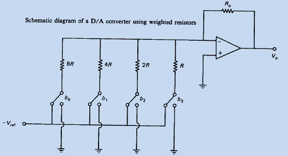
400 Service Wiring Diagram Circuit diagram of Digital to Analog converter using DAC 0800. To study the block diagram and working of GSM mobile phone - Posted By. Give the connections as per the circuit diagram shown in Fig1. DAC channel block diagram 80. In DAC 0808 which among the following is configured as a reference in addition to R-2R ladder and current switches. This chapter deals with Digital to Analog Converters in detail.
This code is fed into the DAC which then supplies the analog equivalent of this digital code V ref 2 into the comparator circuit for comparison with the sampled input voltageIf this analog voltage exceeds V in then the comparator causes the SAR to reset this bit.
Dc To Ac Transformer Wiring Diagram DAC pins 81. The data or information that we perceive in real world exists in analog form while the digital devices such as cellphone calculator computer can only understand a data signal in digital domain. The successive approximation register is initialized so that the most significant bit MSB is equal to a digital 1. Configurations Digital to analog block to generate analog signals with the maximum of 2 channels Channel1 pin A4. Simulink - DAC DAC block can be used to read data 82.
Digital to Analog Converter DAC Types Working Block Diagram Applications.
50s Wiring Diagram Schematic Block and Connection Diagrams Continued Ordering Information ACCURACY OPERATING TEMPERATURE RANGE N PACKAGE N16A Note 1 SO PACKAGE M16A 8-bit 0CTA75C DAC0808LCN MC1408P8 DAC0808LCM Note 1. Answer to Draw the block diagram of a 6-bit SiGe HBT distributed DAC driver with 3Vpp swing per side assuming that there are 7 DA. Signals are mainly classified into two types ie. The block diagram of DAC is shown in the. Switch on the power supply. The successive approximation register is initialized so that the most significant bit MSB is equal to a digital 1.
Is the least efficient diagram among the electrical wiring diagram.
1974 Corvette Radio Wiring Diagram The block diagram of DAC is shown in the. To study the block diagram and working of GSM mobile phone Page Link. The block diagram of DAC is shown in the. This is a major drawback which is eliminated in modern DAC to make them work from a single power source. Pin digram block diagram of dac0800 The DAC0800 is an 8-bit high speed current output DAC with a typical settling time conversion time of 100 ns.
Block diagram of the 1-Digit Voltmeter.
P 32 Workhorse Wiring Diagram ü It produces complementary current output which can be converted to voltage by using simple resistor load. Switch on the power supply. Pin digram block diagram of dac0800 The DAC0800 is an 8-bit high speed current output DAC with a typical settling time conversion time of 100 ns. DAC channel block diagram 80. Variable-precision DSP architecture with hardened floating-point operators provides multiple design benefits. Analog Devices is a global leader in the design and manufacturing of analog mixed signal and DSP integrated circuits to help solve the toughest engineering challenges.
Observe the corresponding output voltage and compare with the theoretical value.
Arduino Uno Diagram To Wire Variable-precision DSP architecture with hardened floating-point operators provides multiple design benefits. Configurations Digital to analog block to generate analog signals with the maximum of 2 channels Channel1 pin A4. A Digital to Analog Converter DAC converts a digital input signal into an analog output signal. Digital to Analog converter Can be configured to 8 or 12 bit mode. - Published on 24 Nov 15.
Eight digital inputs are given to the chip and are supposed to be in order from MSB to LSB.
Vaa21 Relay Wiring Diagram DAC pins 81. Initially the DAC Reference Voltage is set to zero which is smaller than the Analog Input therefore the Comparator outputs a signal to enable the Clock Generator. The successive approximation register is initialized so that the most significant bit MSB is equal to a digital 1. Circuit diagram of Digital to Analog converter using DAC 0800. Is the least efficient diagram among the electrical wiring diagram. Mower Starter Generator Wiring Diagram It is far more helpful as a reference guide if anyone wants to know about the homes electrical system.
Eight digital inputs are given to the chip and are supposed to be in order from MSB to LSB.
Deutz Engine Diagram Model Bf4m1013ec Generator DAC pins 81. A Digital to Analog Converter DAC converts a digital input signal into an analog output signal. Dac in 8051 theory dac0800 interfacing with 8051 suare wave programe of 8051 to dac 0800 information on interfacing dac using parallel ports using 8051 Title. Is the least efficient diagram among the electrical wiring diagram. Eight digital inputs are given to the chip and are supposed to be in order from MSB to LSB.
A Digital to Analog Converter DAC converts a digital input signal into an analog output signal.
1994 Jeep Cherokee Headlight Wiring Diagram DAC0800DAC0802 8-Bit Digital-to-Analog Converters June 1999 DAC0800DAC0802 8-Bit Digital-to-Analog Converters General Description The DAC0800 DAC0802 DAC0800C and DAC0802C are a direct replacement for the DAC-08 DAC-08A DAC-08C The DAC0800 series are monolithic 8-bit high-speed and DAC-08H respectively. Block and Connection Diagrams Continued Ordering Information ACCURACY OPERATING TEMPERATURE RANGE N PACKAGE N16A Note 1 SO PACKAGE M16A 8-bit 0CTA75C DAC0808LCN MC1408P8 DAC0808LCM Note 1. This code is fed into the DAC which then supplies the analog equivalent of this digital code V ref 2 into the comparator circuit for comparison with the sampled input voltageIf this analog voltage exceeds V in then the comparator causes the SAR to reset this bit. Home Category Electronic Engineering MCQ questions. The successive approximation register is initialized so that the most significant bit MSB is equal to a digital 1. DAC pins 81.
Wide bandwidth high performance low power flexible.
Wiring Diagram Ford Mondeo Analog Devices is a global leader in the design and manufacturing of analog mixed signal and DSP integrated circuits to help solve the toughest engineering challenges. It produces complementary current output which can be converted to voltage by using simple resistor load. Provide the required digital input through the switches as indicated in tabular column. DAC channel block diagram 80. Is the least efficient diagram among the electrical wiring diagram.
The data or information that we perceive in real world exists in analog form while the digital devices such as cellphone calculator computer can only understand a data signal in digital domain.
Lamborghini Urraco Wiring Diagram DAC0800DAC0802 8-Bit Digital-to-Analog Converters June 1999 DAC0800DAC0802 8-Bit Digital-to-Analog Converters General Description The DAC0800 DAC0802 DAC0800C and DAC0802C are a direct replacement for the DAC-08 DAC-08A DAC-08C The DAC0800 series are monolithic 8-bit high-speed and DAC-08H respectively. Signals are mainly classified into two types ie. The block diagram of DAC is shown in the. Block and Connection Diagrams Continued Ordering Information ACCURACY OPERATING TEMPERATURE RANGE N PACKAGE N16A Note 1 SO PACKAGE M16A 8-bit 0CTA75C DAC0808LCN MC1408P8 DAC0808LCM Note 1. Dac in 8051 theory dac0800 interfacing with 8051 suare wave programe of 8051 to dac 0800 information on interfacing dac using parallel ports using 8051 Title. For single supply operation refer to AN-1525.
The successive approximation register is initialized so that the most significant bit MSB is equal to a digital 1.
House Wiring Diagram Wikipedia Give the connections as per the circuit diagram shown in Fig1. Block and Connection Diagrams Continued Ordering Information ACCURACY OPERATING TEMPERATURE RANGE N PACKAGE N16A Note 1 SO PACKAGE M16A 8-bit 0CTA75C DAC0808LCN MC1408P8 DAC0808LCM Note 1. Answer to Draw the block diagram of a 6-bit SiGe HBT distributed DAC driver with 3Vpp swing per side assuming that there are 7 DA. A Digital to Analog Converter DAC converts a digital input signal into an analog output signal. Provide the required digital input through the switches as indicated in tabular column.
Switch on the power supply.
Ford Wiper Wiring Diagram The SOIC package pin numbers differ from that of the PDIP package. Pin digram block diagram of dac0800 The DAC0800 is an 8-bit high speed current output DAC with a typical settling time conversion time of 100 ns. Analog Devices is a global leader in the design and manufacturing of analog mixed signal and DSP integrated circuits to help solve the toughest engineering challenges. Is the least efficient diagram among the electrical wiring diagram. DAC0800DAC0802 8-Bit Digital-to-Analog Converters June 1999 DAC0800DAC0802 8-Bit Digital-to-Analog Converters General Description The DAC0800 DAC0802 DAC0800C and DAC0802C are a direct replacement for the DAC-08 DAC-08A DAC-08C The DAC0800 series are monolithic 8-bit high-speed and DAC-08H respectively. DAC0802C are a direct replacement for the DAC-08 DAC-08ADAC-08Cand DAC-08Hrespectively.
- Published on 24 Nov 15.
Murray Riding Mower Carburetor Diagram Pin digram block diagram of dac0800 The DAC0800 is an 8-bit high speed current output DAC with a typical settling time conversion time of 100 ns. - Published on 24 Nov 15. Block diagram of the 1-Digit Voltmeter. This chapter deals with Digital to Analog Converters in detail. Pin digram block diagram of dac0800 The DAC0800 is an 8-bit high speed current output DAC with a typical settling time conversion time of 100 ns.
Situs ini adalah komunitas terbuka bagi pengguna untuk berbagi apa yang mereka cari di internet, semua konten atau gambar di situs web ini hanya untuk penggunaan pribadi, sangat dilarang untuk menggunakan artikel ini untuk tujuan komersial, jika Anda adalah penulisnya dan menemukan gambar ini dibagikan tanpa izin Anda, silakan ajukan laporan DMCA kepada Kami.
Jika Anda menemukan situs ini baik, tolong dukung kami dengan membagikan postingan ini ke akun media sosial seperti Facebook, Instagram dan sebagainya atau bisa juga save halaman blog ini dengan judul Block Diagram Of Dac 0800 dengan menggunakan Ctrl + D untuk perangkat laptop dengan sistem operasi Windows atau Command + D untuk laptop dengan sistem operasi Apple. Jika Anda menggunakan smartphone, Anda juga dapat menggunakan menu laci dari browser yang Anda gunakan. Baik itu sistem operasi Windows, Mac, iOS, atau Android, Anda tetap dapat menandai situs web ini.