Oppo F1s Pcb Diagram - Jika kamu sedang mencari artikel Oppo F1s Pcb Diagram terlengkap, berarti kamu telah berada di blog yang benar. Setiap artikel dibahas secara mendetail dengan penyajian bahasa yang ringan dimengerti bagi orang awam sekalipun. itulah sebabnya web ini banyak diminati para blogger dan pembaca online. Yuk langsung aja kita simak pembahasan Oppo F1s Pcb Diagram berikut ini.
Oppo F1s Pcb Diagram. Therere some OPPO Mobile Phone Schematic Diagrams PDF above the page. 64 GB Motherboard PCB Module Quality. Oppo F1S Series Service Manualdoc. OPPO R2001 Schematic Layout Diagrams. Diagram Oppo A57 Circuit Diagram Full Version Hd Quality Circuit Diagram Pischematic2b Angelux It Diagram Oppo A57 Circuit Diagram Full Version Hd Quality Circuit Diagram Pischematic2b Angelux It.
Farmall M Spark Plug Wiring Diagram PCB Layouts diagrams. See more ideas about smartphone repair phone solutions mobile tricks. Oppo F1s Android smartphone. OPPO A51F Schematics pcb lay outpart04rar 2930 KB 583 views OPPO A51F Schematics pcb lay outpart05rar 2896 KB 585 views The Following 7 Users Say Thank You to d-Artigo For This Useful Post. Therere some OPPO Mobile Phone Schematic Diagrams PDF above the page. Best Mobile Phone All Mobile Phones Mobile Phone Repair Handwriting Examples Android Tutorials Android Hacks Apple Iphone Covers Oppo F1s Iphone Repair.
Aug 14 2019 - Explore pcv hdns board Oppo on Pinterest.
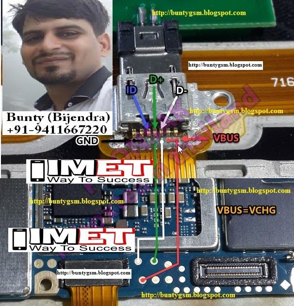
Wiring Diagram Renault 18 Break Reading Oppo F1s Schematic Diagrams is not a hard task to do schematic diagrams are a big help to cellphone-repair especially when working on or tracing lines and finding where particular components mounted on a PCB board. Please need a3s. Download Oppo F1s Schematic Diagram And Service Manual Full Pack Free. Oppo Joy3-A11W-Schematic Diagram pdf Oppo N1-schematics diagram-pcb-layoutOppo-A11w-Joy3-Schematic-Layout-Diagrams pdf OPPO-A51F-Schematic diagram pdf OPPO-A51W-Schematic diagram pdf OPPO-F1-Schematic diagram pdf Oppo-F1s-Service-ManualOppo-Finder-3X905-Schematic-Diagram pdf OPPO-NEO7-A33W-Schematic diagram pdf Oppo-Neo51201-Schematic. Oppo F1s Charging Not Working Problem Solution 100. Download Huawei Honor 8x Schematic Diagram And Service Manual Oppo F1s Display Light Solution In 2020 Oppo F1s Light Display Solutions.
Features 55 display MT6755 or MTK7650 chipset 13 MP primary camera 16 MP front camera 3075 mAh battery 64 GB storage 4 GB RAM Corning.
Peugeot Partner 1 4 Wiring Diagram OPPO r1001 Schematic Layout Diagrams. PCB Diagram of Mobile Phone Free Downloading Websites Most of us already know how to download free schematics from the internet. MattyJohn July 2 2019 at 424 AM. OPPO r1001 Schematic Layout Diagrams. F1s nya gan.
Oppo Neo 7 A33w Schematic Layout Diagrams.
Lincoln 300d Wiring Diagram In case of no s. Download Oppo F1s Schematic Diagram And Service Manual Full Pack Free. Microsoft Word Document 164 MB. Oppo F1s 2CA001-SC PCB Layout Oppo F1s A1601 Schematic Diagram مخطط أوبو F1s A1601 Oppo Reno 2AD066-0 PCB Teardown تشريح أوبو Reno-----Huawei Honor 20 HL1YALEM01 PCB Teardown تشريح هواوي Honor 20 Huawei Honor 9i HL4LDDM PCB Layout. 10 Working DaysShipping MethodsPlease do note that we ship all orders through Bluedart FedEx DTDC Aramex Professional and Overnite courier Service. Please need a3s.
Aug 14 2019 - Explore pcv hdns board Oppo on Pinterest.
Cadillac Cts Engine Diagram Oppo A11w joy 3Schematics Diagrams PDF. The OPPO brand began its history in 2004. 10 Days Delivery. MattyJohn July 2 2019 at 424 AM. OPPO R2001 Schematic Layout Diagrams.
Unknown May 29 2019 at 336 AM.
Cat 5 Pinout Diagram PCB Diagram of Mobile Phone Free Downloading Websites Most of us already know how to download free schematics from the internet. Oppo F1s Charging Not Working Problem Solution 100. Such schematic diagrams are a very useful and very important guide in every cellphone technician. Feb 11 2020 - Oppo F1S Display Light Solution check above all the paths and if one tracks of them are missing apply jumpers. Download Images Library Photos and Pictures. Oppo F1s Schematic Diagram helps you identify the mobile phone circuit boards original parts and components.
Oppo F1s Schematic Diagram helps you identify the mobile phone circuit boards original parts and components.
Wiring Diagram Inverter Feb 11 2020 - Oppo F1S Display Light Solution check above all the paths and if one tracks of them are missing apply jumpers. Oppo Neo 5 1201 Schematic Layout Diagrams. Oppo F1s Part. In case of no s. OPPO r1001 Schematic Layout Diagrams.
OPPO user manuals PDF.
Rj9 To 3 5mm Wiring Diagram Download Images Library Photos and Pictures. OPPO R821 Schematic. MattyJohn July 2 2019 at 424 AM. Oppo F1s Charging Not Working Problem Solution 100. Therere some OPPO Mobile Phone Schematic Diagrams PDF above the page. Oppo F1s Part.
OPPO R819 Schematic Layout Diagrams.
Acura Tl Wiring Diagram F1s nya gan. Oppo Joy3-A11W-Schematic Diagram pdf Oppo N1-schematics diagram-pcb-layoutOppo-A11w-Joy3-Schematic-Layout-Diagrams pdf OPPO-A51F-Schematic diagram pdf OPPO-A51W-Schematic diagram pdf OPPO-F1-Schematic diagram pdf Oppo-F1s-Service-ManualOppo-Finder-3X905-Schematic-Diagram pdf OPPO-NEO7-A33W-Schematic diagram pdf Oppo-Neo51201-Schematic. Download Images Library Photos and Pictures. F1s nya gan. Please need a3s.
Also you will find the Block Diagram format File PDF you can use this schematic for repair damage by hardware to identify ways of a block diagram to make jumper trick to find the component layout Schematic And Block Diagram Troubleshooting.
197C10 Wiring Diagram OPPO user manuals PDF. In 2005 OPPO launched the first MP3 player in the Chinese market and the first model of a high-end DVD player in the US 2006 - Launch of the category of portable video players 2008 - release of the first mobile phone 2009 - OPPO went to Thailand. PCB Diagram of Mobile Phone Free Downloading Websites Most of us already know how to download free schematics from the internet. Disassembly assembly manuals See also. Diagram Oppo A37f Schematic Diagram Full Version Hd Quality Schematic Diagram Cbschematic2b Angelux It Diagram Oppo A33w Circuit Diagram Full Version Hd Quality Circuit Diagram Boacorhoiapomeeryomc Gsdportotorres It Diagram Oppo A37 Pcb Diagram Full Version Hd Quality Pcb Diagram Pdfxbaleyl Palazzojuvalta It Diagram Oppo A37 Motherboard Diagram Full. OPPO R819 Schematic Layout Diagrams.
Disassembly assembly manuals See also.
2000 Trooper Transmission Wiring Diagram OPPO R2001 Schematic Layout Diagrams. PCB Layouts diagrams. Disassembly assembly manuals See also. OPPO R821 Schematic. Oppo Joy3-A11W-Schematic Diagram pdf Oppo N1-schematics diagram-pcb-layoutOppo-A11w-Joy3-Schematic-Layout-Diagrams pdf OPPO-A51F-Schematic diagram pdf OPPO-A51W-Schematic diagram pdf OPPO-F1-Schematic diagram pdf Oppo-F1s-Service-ManualOppo-Finder-3X905-Schematic-Diagram pdf OPPO-NEO7-A33W-Schematic diagram pdf Oppo-Neo51201-Schematic.
PCB Diagram of Mobile Phone Free Downloading Websites Most of us already know how to download free schematics from the internet.
197Skylark Wiring Diagram Oppo Schematics Servis Manual Download Free OPPO CIRCUIT DIAGRAM DOWNLOAD FREE - BEST SITE. Oppo F1s 2CA001-SC PCB Layout Oppo F1s A1601 Schematic Diagram مخطط أوبو F1s A1601 Oppo Reno 2AD066-0 PCB Teardown تشريح أوبو Reno-----Huawei Honor 20 HL1YALEM01 PCB Teardown تشريح هواوي Honor 20 Huawei Honor 9i HL4LDDM PCB Layout. Unknown May 29 2019 at 336 AM. Oppo F1 Schematic Layout Diagrams. Oppo Joy3-A11W-Schematic Diagram pdf Oppo N1-schematics diagram-pcb-layoutOppo-A11w-Joy3-Schematic-Layout-Diagrams pdf OPPO-A51F-Schematic diagram pdf OPPO-A51W-Schematic diagram pdf OPPO-F1-Schematic diagram pdf Oppo-F1s-Service-ManualOppo-Finder-3X905-Schematic-Diagram pdf OPPO-NEO7-A33W-Schematic diagram pdf Oppo-Neo51201-Schematic. Please need a3s.
Oppo Joy3-A11W-Schematic Diagram pdf Oppo N1-schematics diagram-pcb-layoutOppo-A11w-Joy3-Schematic-Layout-Diagrams pdf OPPO-A51F-Schematic diagram pdf OPPO-A51W-Schematic diagram pdf OPPO-F1-Schematic diagram pdf Oppo-F1s-Service-ManualOppo-Finder-3X905-Schematic-Diagram pdf OPPO-NEO7-A33W-Schematic diagram pdf Oppo-Neo51201-Schematic.
Vw 1600 Bus Engine Tin Diagram OPPO R815 Schematic Layout Diagrams. Download Huawei Honor 8x Schematic Diagram And Service Manual Oppo F1s Display Light Solution In 2020 Oppo F1s Light Display Solutions. Features 55 display MT6755 or MTK7650 chipset 13 MP primary camera 16 MP front camera 3075 mAh battery 64 GB storage 4 GB RAM Corning. Oppo Joy3-A11W-Schematic Diagram pdf Oppo N1-schematics diagram-pcb-layoutOppo-A11w-Joy3-Schematic-Layout-Diagrams pdf OPPO-A51F-Schematic diagram pdf OPPO-A51W-Schematic diagram pdf OPPO-F1-Schematic diagram pdf Oppo-F1s-Service-ManualOppo-Finder-3X905-Schematic-Diagram pdf OPPO-NEO7-A33W-Schematic diagram pdf Oppo-Neo51201-Schematic. Oppo F1s Charging Not Working Problem Solution 100.
215063_SC 215063_SC_2 215063_SB.
Master Power Window Switch Wiring Diagram Oppo Joy3-A11W-Schematic Diagram pdf Oppo N1-schematics diagram-pcb-layoutOppo-A11w-Joy3-Schematic-Layout-Diagrams pdf OPPO-A51F-Schematic diagram pdf OPPO-A51W-Schematic diagram pdf OPPO-F1-Schematic diagram pdf Oppo-F1s-Service-ManualOppo-Finder-3X905-Schematic-Diagram pdf OPPO-NEO7-A33W-Schematic diagram pdf Oppo-Neo51201-Schematic. OPPO A51F Schematics pcb lay outpart04rar 2930 KB 583 views OPPO A51F Schematics pcb lay outpart05rar 2896 KB 585 views The Following 7 Users Say Thank You to d-Artigo For This Useful Post. Oppo F1s Android smartphone. Please need a3s. OPPO R821 Schematic. Oppo Neo 7 A33w Schematic Layout Diagrams.
Download Oppo F1s Schematic Diagram And Service Manual Full Pack Free.
Mo Diagram For Boron In 2005 OPPO launched the first MP3 player in the Chinese market and the first model of a high-end DVD player in the US 2006 - Launch of the category of portable video players 2008 - release of the first mobile phone 2009 - OPPO went to Thailand. Oppo F1s Schematic Diagram helps you identify the mobile phone circuit boards original parts and components. Oppo F1s Android smartphone. 64 GB Motherboard PCB Module Quality. F1s nya gan.
Aug 14 2019 - Explore pcv hdns board Oppo on Pinterest.
2005 F350 Fuse Box Diagram 215063_SC 215063_SC_2 215063_SB. 215063_SC 215063_SC_2 215063_SB. Oppo F1s Schematic Diagram helps you identify the mobile phone circuit boards original parts and components. Oppo F1s Charging Not Working Problem Solution 100. Also you will find the Block Diagram format File PDF you can use this schematic for repair damage by hardware to identify ways of a block diagram to make jumper trick to find the component layout Schematic And Block Diagram Troubleshooting. Unknown May 29 2019 at 336 AM.
Download Images Library Photos and Pictures.
Protege Manual 5 Speed Gear Shift Link Diagram Oppo F1s Android smartphone. The OPPO brand began its history in 2004. OPPO R821 Schematic. OPPO r1001 Schematic Layout Diagrams. Feb 11 2020 - Oppo F1S Display Light Solution check above all the paths and if one tracks of them are missing apply jumpers.
Situs ini adalah komunitas terbuka bagi pengguna untuk mencurahkan apa yang mereka cari di internet, semua konten atau gambar di situs web ini hanya untuk penggunaan pribadi, sangat dilarang untuk menggunakan artikel ini untuk tujuan komersial, jika Anda adalah penulisnya dan menemukan gambar ini dibagikan tanpa izin Anda, silakan ajukan laporan DMCA kepada Kami.
Jika Anda menemukan situs ini baik, tolong dukung kami dengan membagikan postingan ini ke akun media sosial seperti Facebook, Instagram dan sebagainya atau bisa juga simpan halaman blog ini dengan judul Oppo F1s Pcb Diagram dengan menggunakan Ctrl + D untuk perangkat laptop dengan sistem operasi Windows atau Command + D untuk laptop dengan sistem operasi Apple. Jika Anda menggunakan smartphone, Anda juga dapat menggunakan menu laci dari browser yang Anda gunakan. Baik itu sistem operasi Windows, Mac, iOS, atau Android, Anda tetap dapat menandai situs web ini.